Information & Services

Hana Semiconductor (Ayutthaya) is a subsidiary of Hana Microelectronics Public Co., Ltd., specializing in the IC assembly
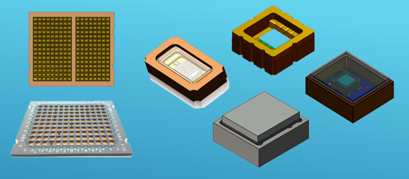
Hana Semiconductor(Ayutthaya) provides a wide range of semiconductor Assembly Services & Full turn-key Service Our packaging capability includes Leaded Packages, Leadless Packages, Laminate Package, Wafer Sort/Dicing Sale Dice Our packaging solutions include System In package(SIP), Multichip Modile(MCM), Cu-Clip, MEMS, ), High Power package, Open Cavity Package & Smart Card Module (RFID) , Thin QFN, Multi-Row/MIS QFN,
We Also provide design service to support Custom Package And package characterization capabilities to help our customers achieve both performance And cost objectives.
Ceramic Substrate
Diesale
Die Types : IC, Emitter, Detector,LED,Diodes, MOSFET, Bumped die,CMOS, BiCMOS, Bipolar
Die Applications : Medical, Commercial, Industrial
Process: Wafer probe – Wafer Backgrind/Saw – Die Inspection, Pick & Place – Pack.
Packing Type : Waffle tray, Wafer ring Or Tape & Reel are available.
Final Testing
- Hana provides semiconductor final test solutions for a variety of devices type including Discrete, Logic & Memory, Mixed-signal, Linear, RF, High voltage isolation, OPTO coupler, Solid state relay and Proximity sensor
- Dedicated test building with over 600 test systems and 500 handlers to provide wide range test of services and meet customer’s device requirement
- New product qualification and sustaining product support by experienced engineering team
- Deliver re-engineering/test conversion solutions to improve test yield, cost reduction and increasing test capacity
- Implemented EMS and factory automation system to deliver robust process control and maximize test throughput
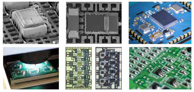
Laminate Package
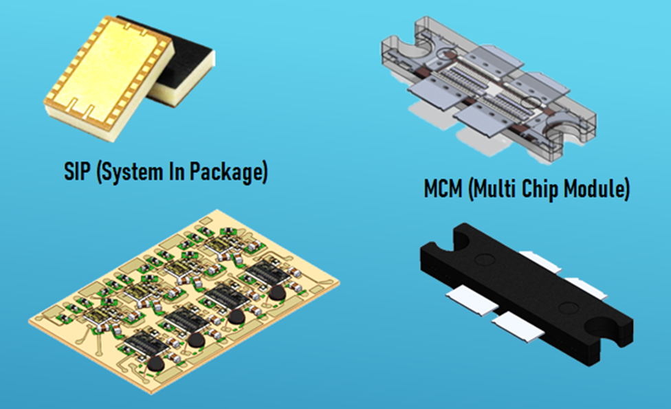
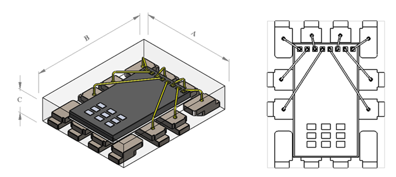
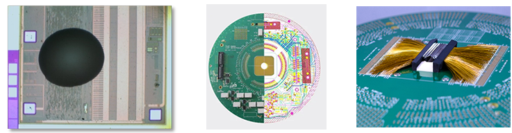
Hana’s Multi-Chip Module (MCM) is an electronic package consisting of multiple integrated circuits (ICs) assembled into a single device. The various components of a MCM are mounted on a substrate and connected to the surface wire bonding. The module can be encapsulated by a plastic molding on Lead frame package/plastic or ceramic Lid on Substrate/Ceramic package. Hana’s System-In-Package (SIP) technology is an 2 or more semiconductor devices. We included both Integrated Circuit (ICs) with Passive components and integration to laminate package.
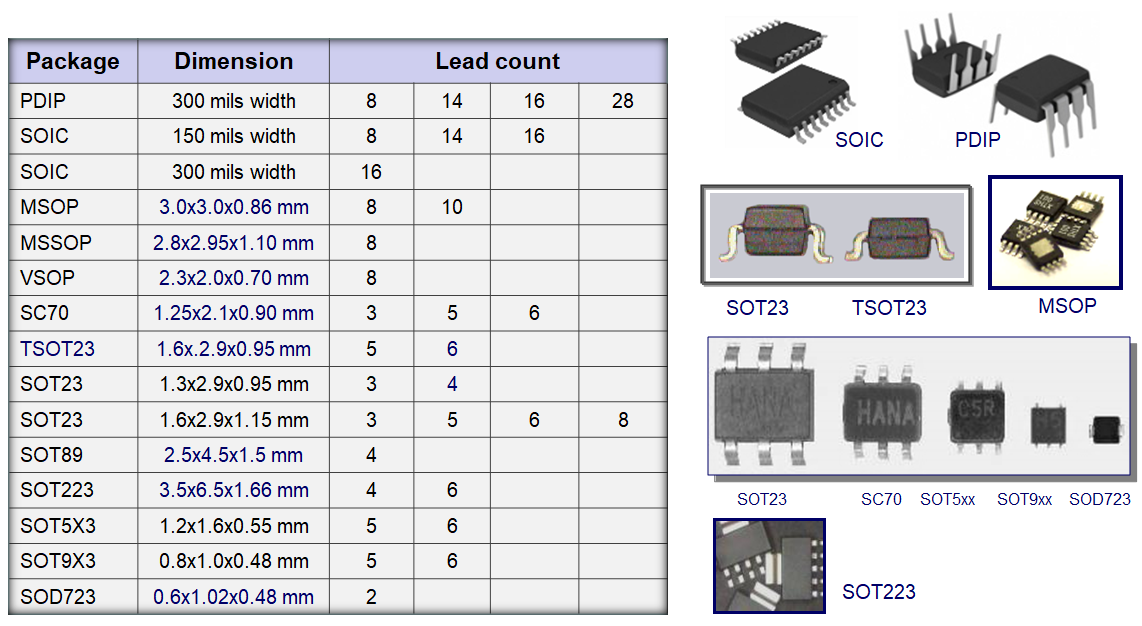
Lead Packages
Package offering for Leaded Package PDIP, SOIC, MSOP. VSOP, SC70, SOT23, SOT223, SOT5X3, SOD723, MSOP
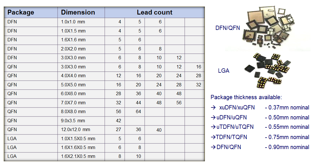
Leadless Packages
Package offering for Leadless Packages QFN/DFN, LGA
Specific body sizes can be tool-up
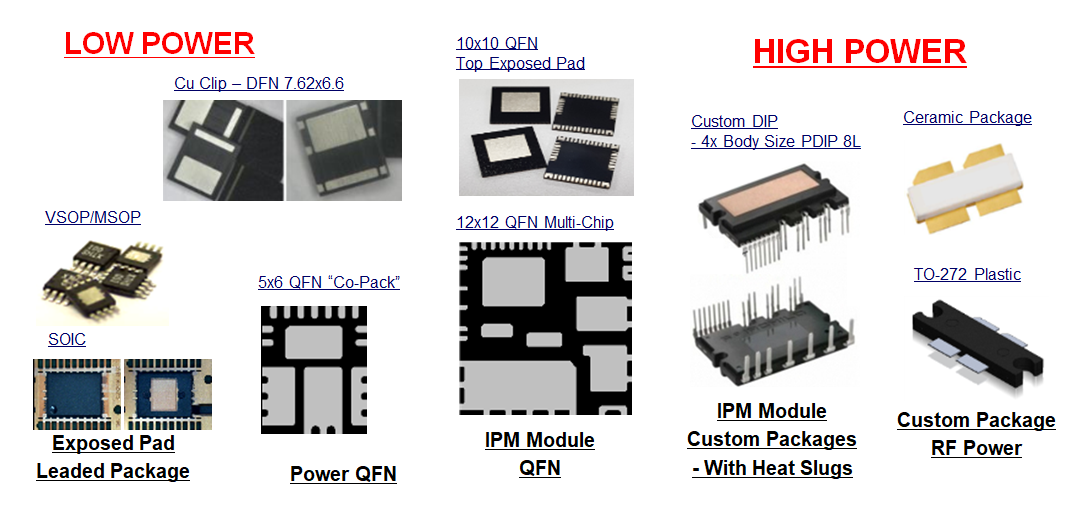
Low High Power Packages
Similar to standard IC molding but design with exposed Pad on Top & Bottom
Wide range Of package options from SOIC, QFN to custom designs
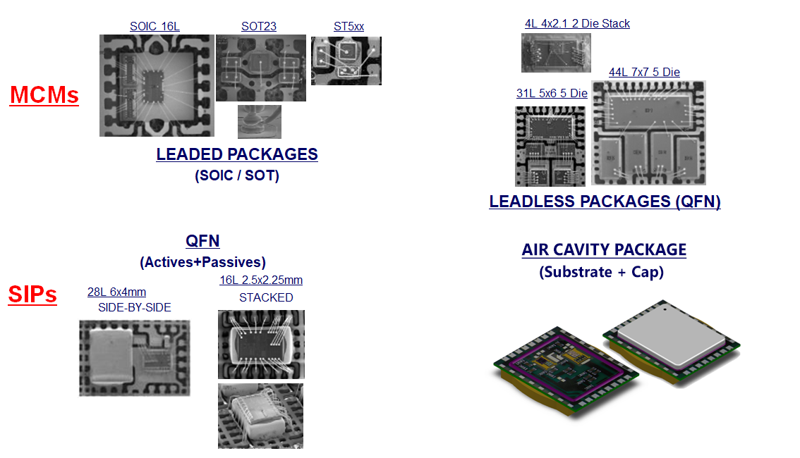
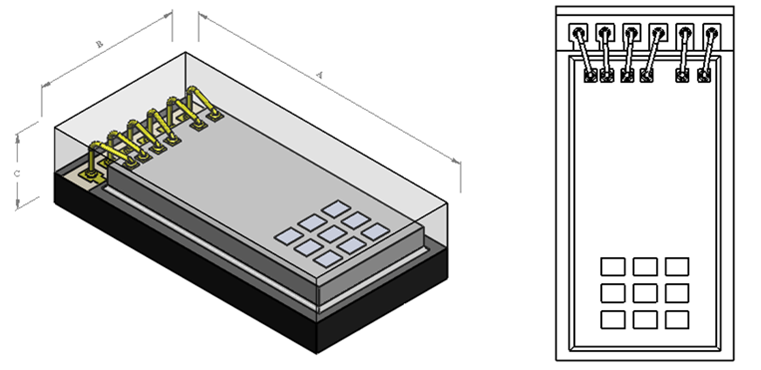
MCMs SIPs Packages (Leaded Leadless)
MCM & SIPs functionality into leaded packages, QFN, & hybrid substrates
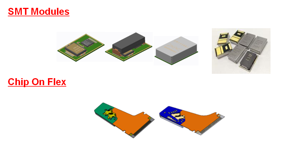
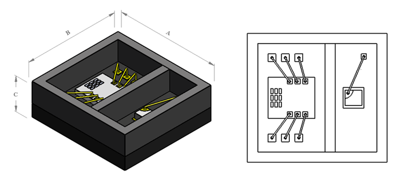
MCMs SIPs Packages (on PCB Flex)
SMT process but finalize as sawn in metal lid or overmold type
SMT on flex substrate, 0201 component sizes
Pick & Place is capable for even smaller 01005 component sizes
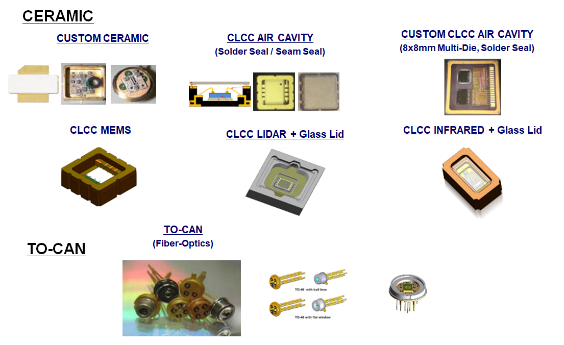
Open Cavity Packages (Ceramics)
Custom ceramic package designs & TO-Can capability
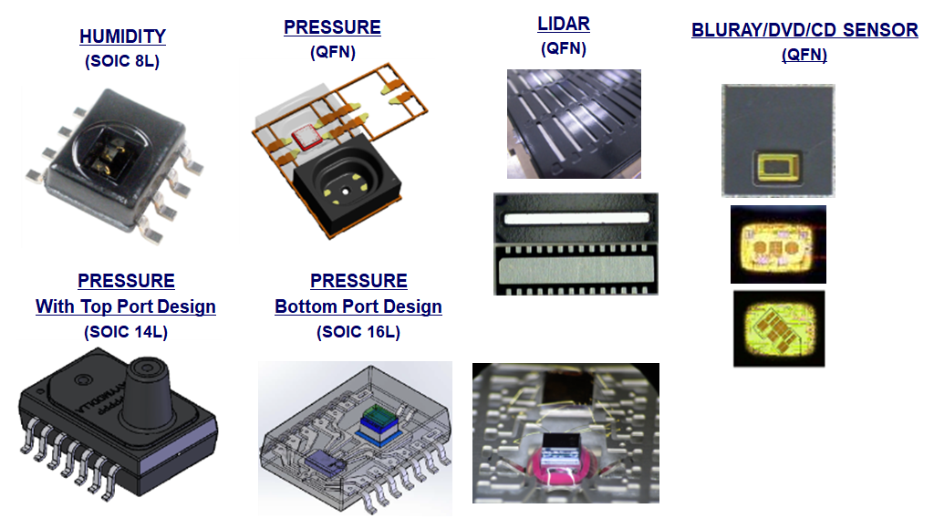
Open Cavity Packages (Plastic)
Similar to standard IC molding but with specific areas opened for the sensor location (plastic package)
Wide range of sensor applications for open cavity or film assist molding
Pressure / humidity / temperature / photodetector apps
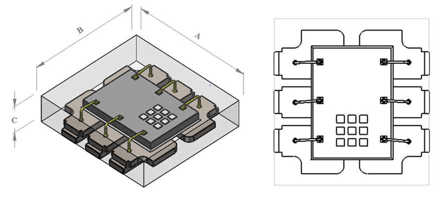
Optical Sensor ODFN
Hana’s optical dual flat non lead (oDFN) is small foot print for light emitter and light detector IC packaging solution. It is custom design from 1.5 to 5.0 mm in width (A) and 2.0 to 5.0 mm in length (B). The standard thickness (C) available are 0.50 and 0.65 mm.
Optical Sensor OLGA
Hana’s optical land grid array (oLGA) is small foot print for light emitter and light detector optical package solution. It is custom design from 1.0 to 5.0 mm in width (B) and 2.0 to 5.0 mm in length (A). The standard thickness (C) available are 0.50 and 0.60 mm.
Optical Sensor OLGA-W
Hana’s optical land grid array with wall (oLGA-W) is small foot print for light emitter and light detector module. It is custom design from 2.5 to 5.0 mm in width (B) and 2.5 to 5.0 mm in length (A). The standard thickness (C) available are 0.90 mm.
Optical Sensor OQFN
Hana’s optical quad flat non lead (oQFN) is small foot print in light emitter and light detector IC packaging solution. It is custom design from 1.5 to 5.0 mm in width (A) and 2.0-5.0 mm in length (B). The standard thickness (C) available are 0.50 and 0.65 mm.
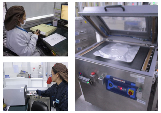
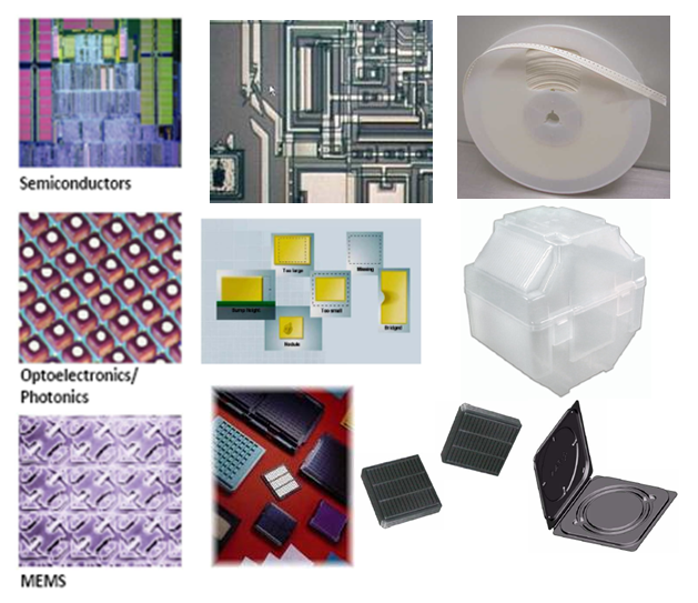
Packing
Hana’s standard packing material covers various IC package type, both leadless and leaded in tube, tape and reel and tray with MSL1-4 capability included dry pack. Full barcode automation system has been implemented for labeling and lot tracking from Finished goods until Ship out.
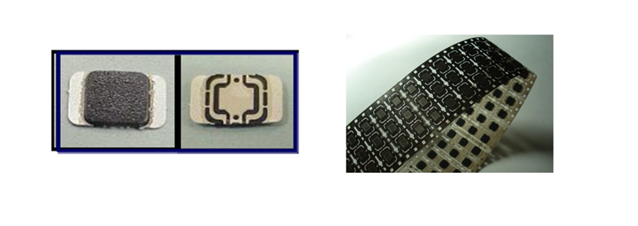
RFID Package
Available in reel-to-reel form
HOA2 with 0.40 mm thickness
HOA4 with 0.33 mm thickness
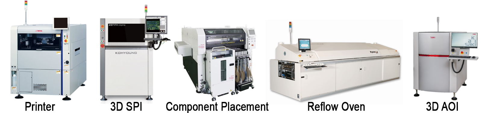
SMT Capability
| Component Size | Min | 01005 (0402 mm) |
| Max | 55 mm x 100 mm | |
| Substrate Size | Min | 50 mm x 50 mm |
| Max | 250 mm x 300 mm | |
| Solder Paste Printing | Accuracy | +/- 10 micron |
| Solder Paste inspection | Type | 3D Inspection (Height / Area / Volumn) |
| Component Placement | Accuracy | +/- 30 micron |
| Reflow Soldering | Max Temperature | 350 Celsius |
| N2 Control | < 100 ppm | |
| AOI | Type | 3D Inspection (Camera Resolution 12 um) |
Test Development Services
Hana has a experienced test team that can help customers develop and customized test programs and procure associated hardware (Load boards, DUT boards, Contactors) to test their semiconductor products on advanced test equipment. Test platform conversion is also offered.
Test Development Stages
- Test Engineering discussion - new device test requirements
- Test project plan milestones
- Test program development
- Engineering Correlation
- Qualification lot testing
- Release internal test procedures
- Mass production
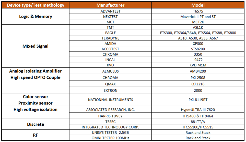
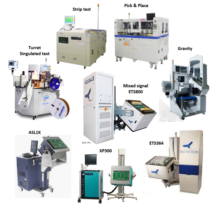
Test Systems
Hana has extensive experience on various tester platforms. Having over 600 test systems and 49 brands of equipment installed in Hana’s test floor gives Hana the capability to test devices types listed below.
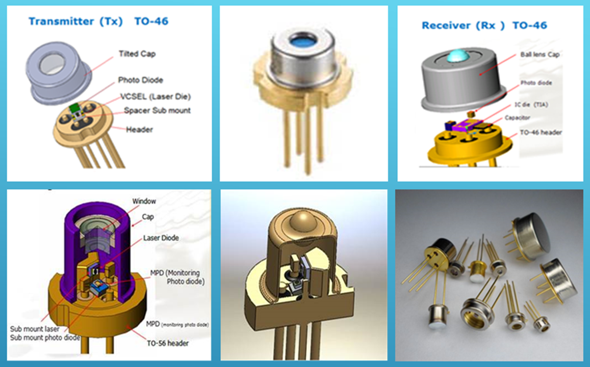
To Can Package
The transistor outline (TO) package family consists of many types of packaging solutions for transistors and similar discrete devices as well as simple IC's with low pin counts. The structures of TO packages vary widely, Hana is focus on Mental Can enclosures as sample package shown.
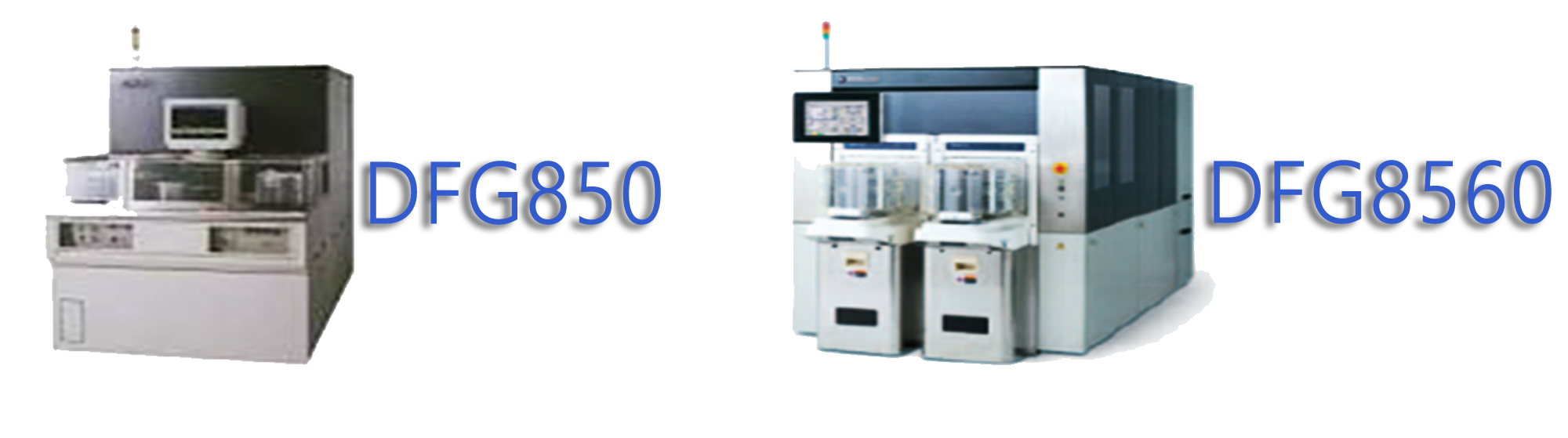
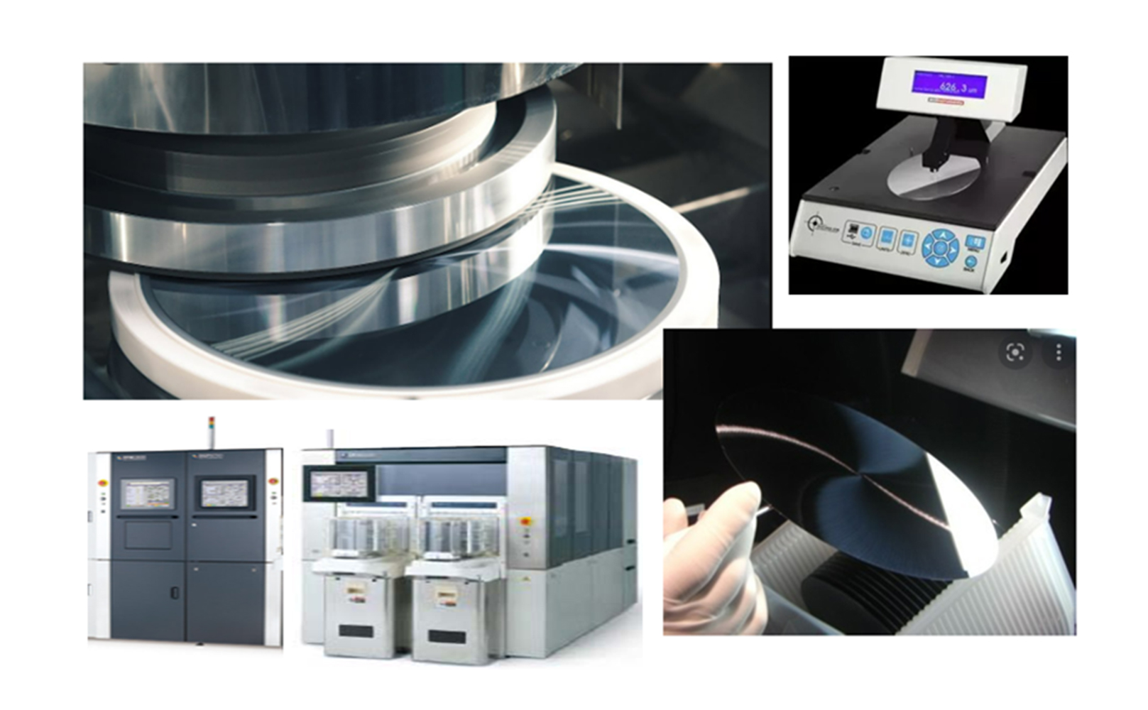
Wafer Back-grinding
| Capability | Current |
|---|---|
| Wafer Type | Silicon : BOPO, BPOA, TMA, CMOS with CUP , Bumped Wafers, Others |
| Standard Wafer : Wafer Diameter/ Thickness | 4”, 5”, 6”, 8” and 12” / 100 um max final thickness |
| Bump Wafer : Wafer Diameter/ Thickness | 8”/ 150-200 um |
| Polishing | PoliGrind Finish with Ra max 2500A (DFG8560/850) |
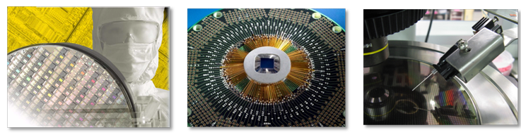

Wafer Sort
Hana can provide electrical wafer sort testing up to 8 inch wafers with multiple Test Sites.
Wafer Sort Service
- Wafer sizes supported up to 8” (200mm)
- Min Die Size 0.38mm x 0.38mm
- Max Die/wafer 400,000 dies
- Ambient/Hot testing up to 150C
- Offline inking
- Communication Protocols Supported: Serial/Parallel/GPIB
- Clean Room environment Class 10k
- OCR, Barcode and Video microscopes available
- Probe card repair and alignment (Done with offsite vendors)
Equipment Capability
| MANUFACTURING | MODEL |
|---|---|
| EG (Electro Glass) | 4090u (200mm) |
| TEL | P8-XL (200mm) |
| TSK | UF200R(200mm) |