
HANA Technologies, Inc.
MICROELECTRONICS ASSEMBLY AND MICRODISPLAYS
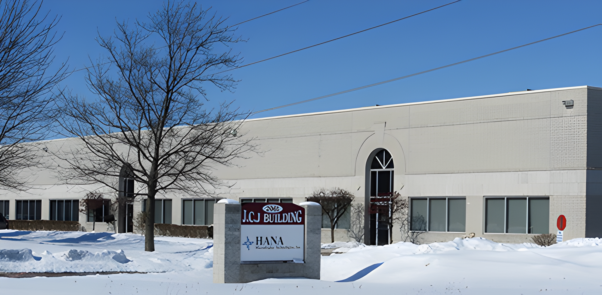
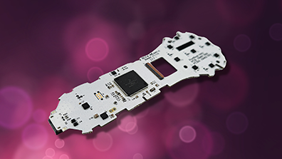
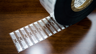
Located in Solon, Ohio, the multi-purpose plant includes the manufacture of Microdisplays (both LC and MEMs-based), three high-speed, roll-to-roll flip-chip RFID inlay lines, and other IC and Microelectronic assembly processes. While it is not an LCD Fab, Wafer Fab, or IC packaging site, the best LCD, wafer fab, and packaging equipment was brought in and customized for unique capabilities. The Ohio site is the US base for Hana’s North American manufacturing efforts, as well as serving the company as an NPI and manufacturing launch site for emerging technologies and products.


